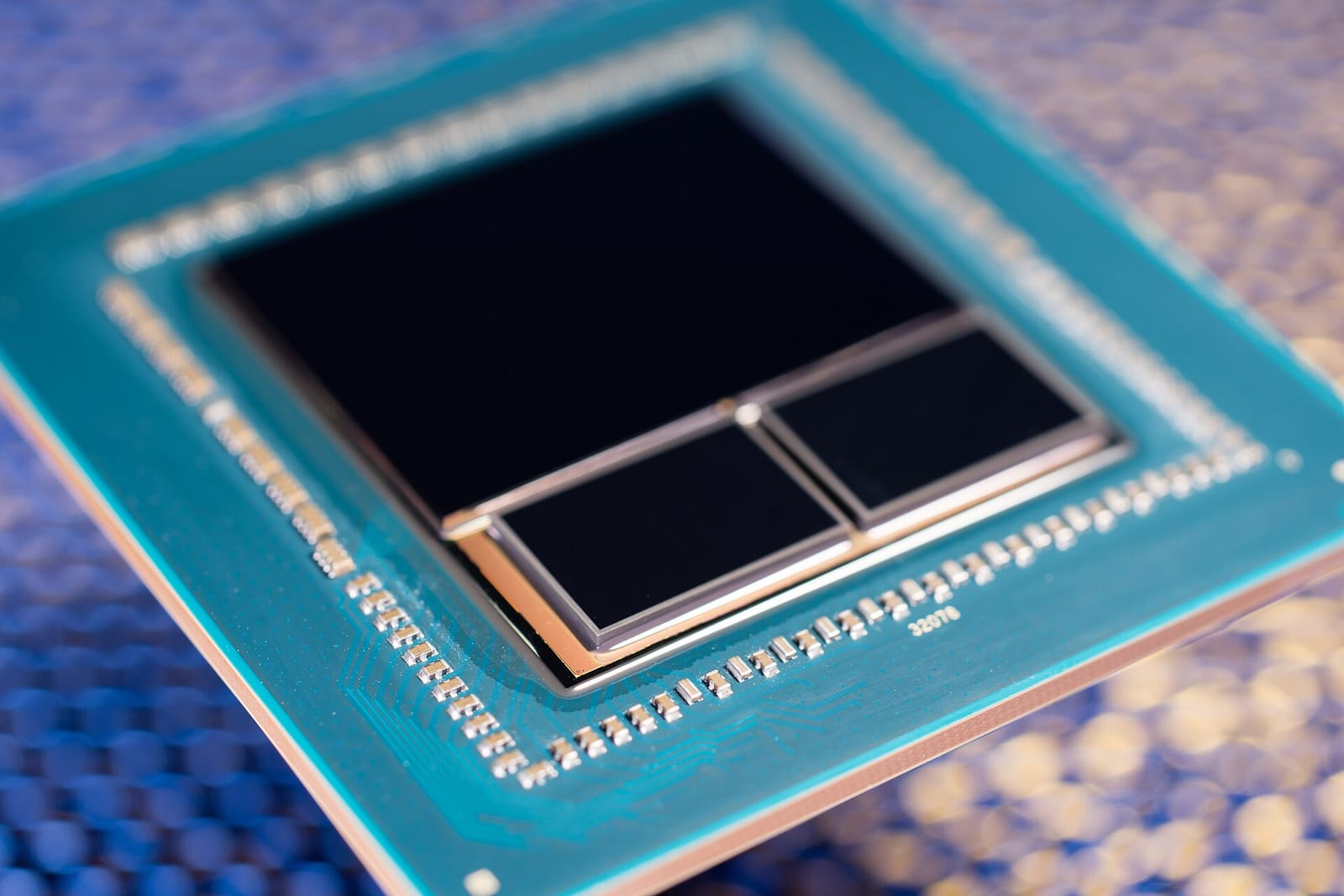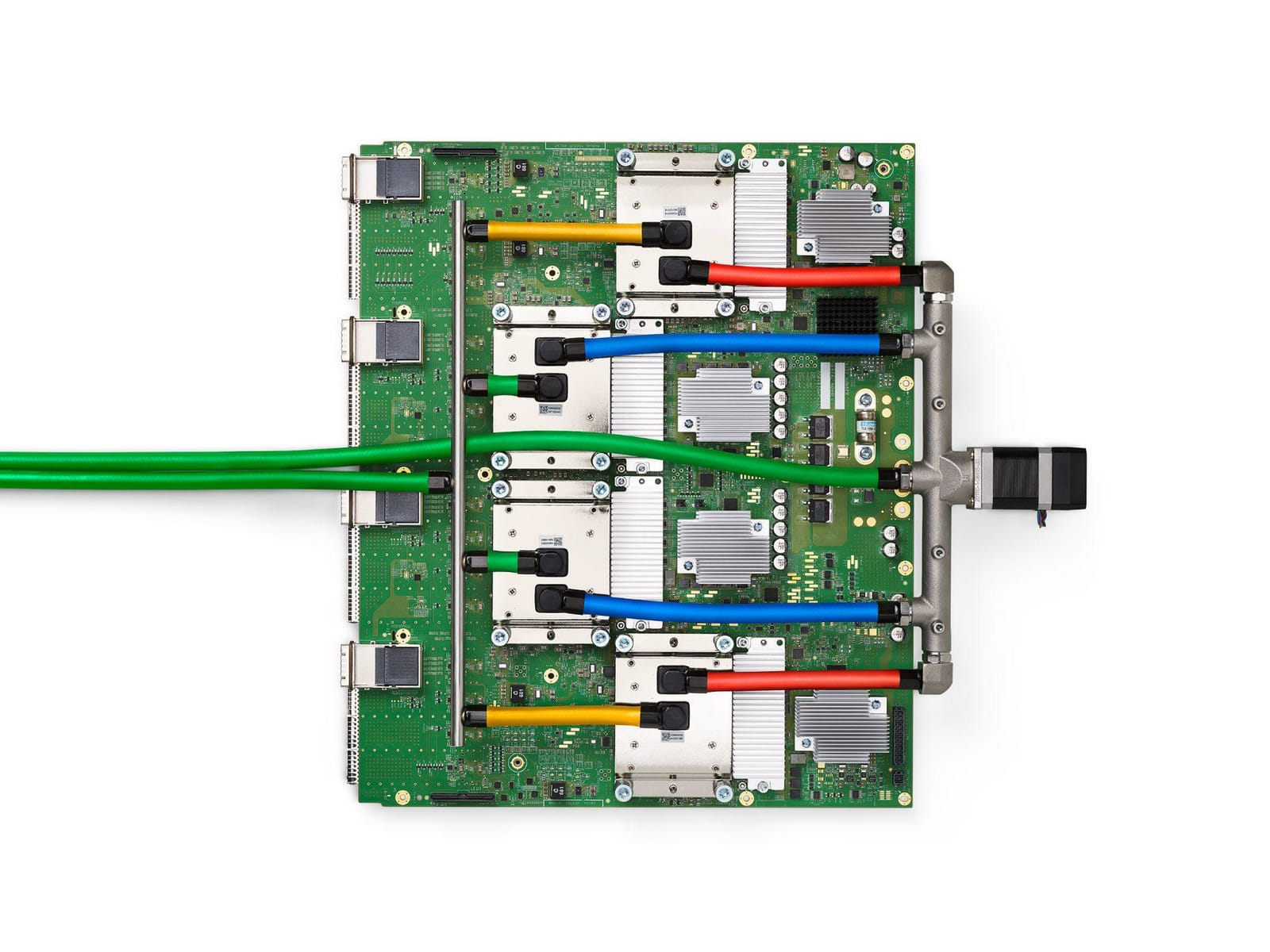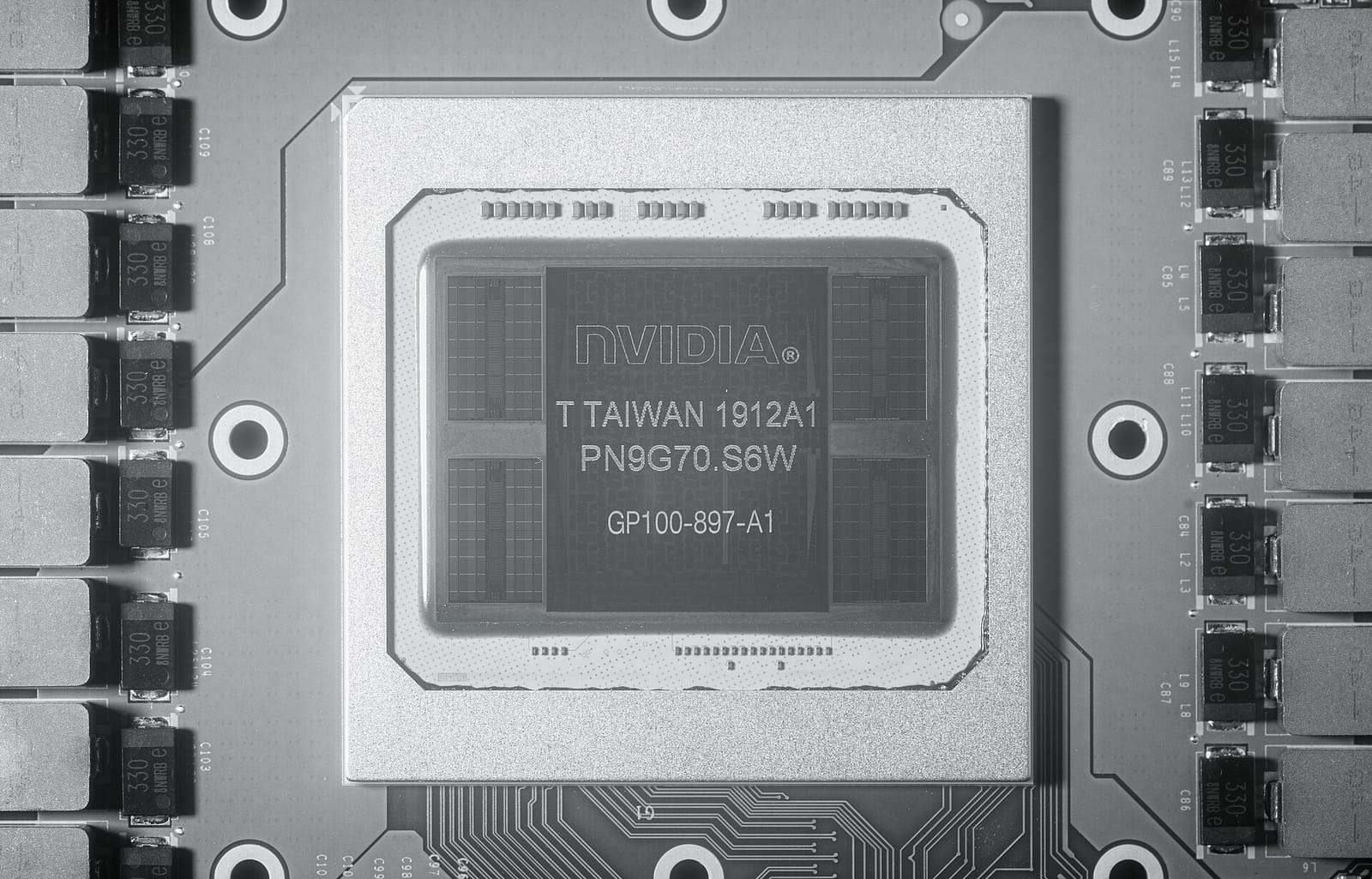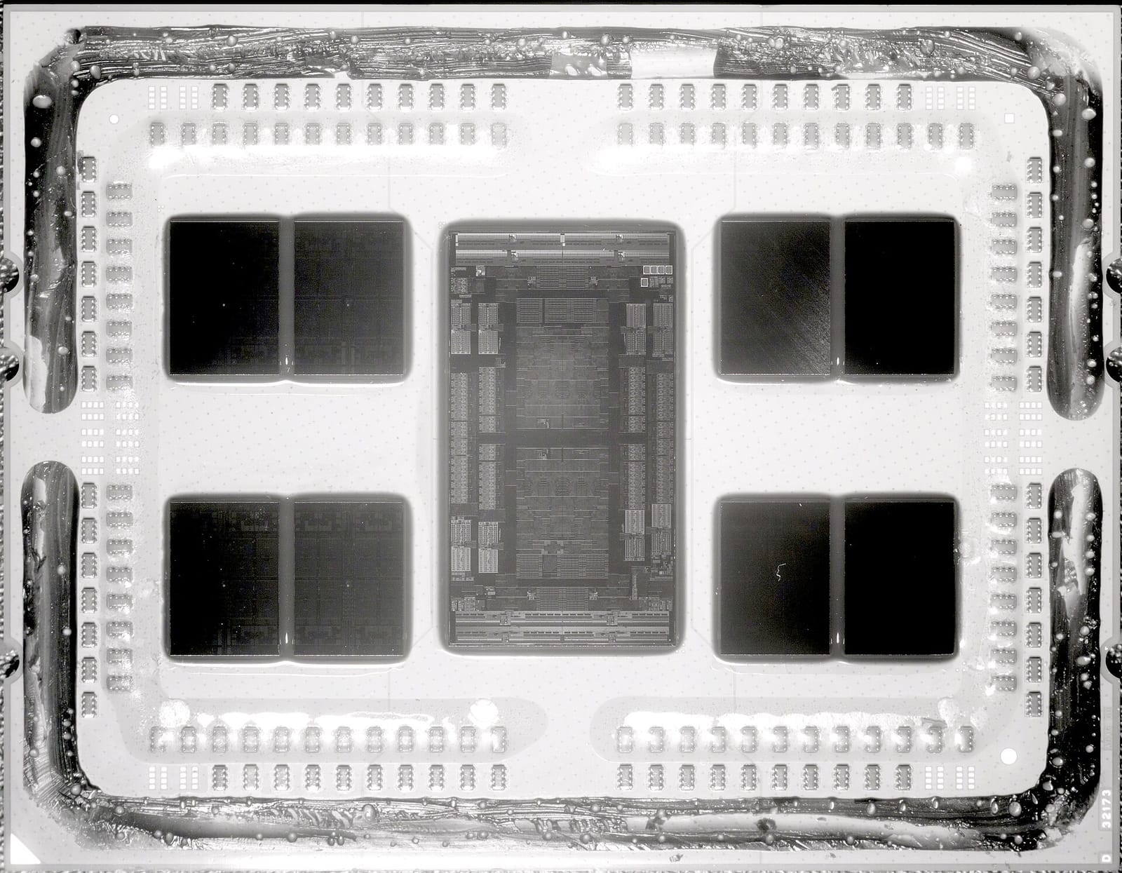
For decades, progress in computing meant putting more transistors on a single piece of silicon. That approach is running into physical and economic limits. Today’s most powerful AI processors are instead built from several smaller pieces of silicon — chiplets — combined with memory in a single package. How those pieces are connected, known as advanced packaging, has become as important as the chips themselves.
Why one big chip is no longer enough
- The reticle limit: lithography machines can only print a chip up to a maximum area in one exposure, roughly 800 square millimetres. The largest AI processors already approach that limit.
- Yields: the bigger a chip, the more likely a manufacturing defect ruins it. Several smaller dies yield far better than one huge one.
- Cost of advanced nodes: not every part of a chip benefits from the newest, most expensive process. Input/output or memory controllers can use older, cheaper nodes.
- Flexibility: chiplets can be mixed and reused across products.
What chiplets are
A chiplet is a die designed to work together with other dies in one package. A processor might combine several compute dies, input/output dies and cache dies, connected by very short, very fast links. To the software, the package behaves like a single chip.
Standards such as UCIe (Universal Chiplet Interconnect Express), backed by a consortium of chipmakers and cloud companies, aim to let chiplets from different vendors work together, much as standard interfaces did for components on circuit boards.
2.5D and 3D packaging
2.5D packaging places dies side by side on a silicon interposer — a thin slab of silicon with dense wiring — that connects them with thousands of fine connections. This is how most AI accelerators connect their compute dies to HBM memory stacks. TSMC’s CoWoS (Chip-on-Wafer-on-Substrate) family is the best-known example and has been central to AI accelerator production.
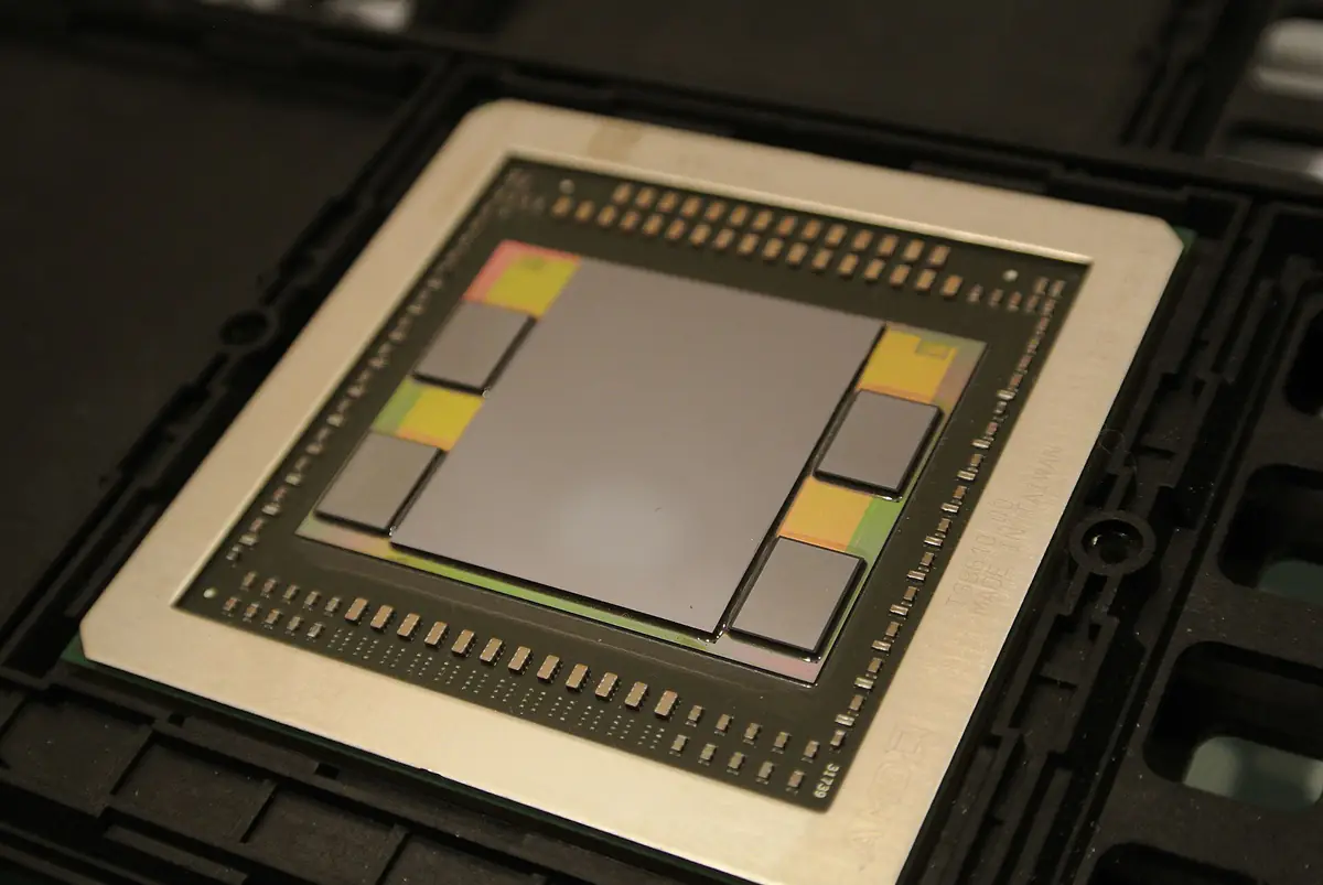
3D packaging stacks dies on top of each other, connecting them vertically. It shortens connections even further and saves area, but makes heat removal harder. HBM itself is a form of 3D stacking.
Why packaging became a bottleneck
During the AI boom, demand for accelerators has outrun the capacity of advanced packaging lines. Even when enough compute dies and memory are available, chips cannot ship until they are packaged. Foundries and packaging companies have been expanding capacity rapidly, and packaging capacity has become a closely watched indicator of how many AI chips the industry can deliver.
Benefits and trade-offs
Benefits: larger effective chips than one die allows, better yields, mixing process nodes, faster product variation.
Trade-offs: complex design and testing, heat concentration, communication between dies that is slower and more power-hungry than within a single die, and dependence on a small number of packaging suppliers.
What it means
AI chip competition is increasingly about system design: how many dies, how much memory, how they are connected and cooled. Understanding packaging helps explain supply shortages, product roadmaps and why big tech builds its own chips.
An analogy
Think of a single large chip as a whole city built on one plot of land: one flaw ruins everything. Chiplets are neighbourhoods built separately and connected by high-speed roads — advanced packaging — so each can be built where it is cheapest and best.
What to watch next
- Expansion of CoWoS and other advanced packaging capacity.
- Adoption of UCIe for multi-vendor chiplets.
- 3D-stacked logic and memory in AI accelerators.
- Co-packaged optics for faster chip-to-chip links.
Key takeaways
- The largest AI processors are limited by the reticle size and manufacturing yields.
- Chiplets split a processor into smaller dies combined in one package.
- 2.5D packaging connects dies and HBM on a silicon interposer; 3D stacks them vertically.
- Advanced packaging capacity has become a bottleneck for AI chip supply.
- AI chip competition is increasingly about the whole package and system.
Frequently asked questions
What is CoWoS?
TSMC’s family of 2.5D packaging technologies that place compute dies and memory side by side on an interposer; widely used for AI accelerators.
Are chiplets slower than a single chip?
Links between dies are slower and use more power than on-die wiring, but advanced packaging makes them fast enough for most designs.
Why do chiplets matter for consumers?
They help make processors cheaper and more varied, and are used in many desktop and server CPUs as well as AI chips.